
Blanket Wafers & Thin Film Deposition
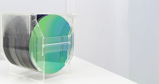
Philtech provides deposition and plating services for semiconductor, insulating, metal, and other films, and supplies film-coated wafers.
We can handle everything from substrate sourcing to film deposition. You can also request just the deposition step in your manufacturing or development process while handling the preceding and subsequent steps yourself. Cutting after deposition is also available.
Discuss Your Blanket Wafer & Deposition Requirements
Contact UsApplications of Blanket Wafers
Substrates, Film Materials & Deposition Methods
Supported Substrates
| Item | Details |
|---|---|
| Supported Substrate Sizes | 4-inch (100 mm), 6-inch (150 mm), 8-inch (200 mm), 12-inch (300 mm) |
| Supported Substrate Materials | In addition to silicon wafers, we can process compound semiconductor wafers, quartz and glass substrates, ceramics, chips, rectangular substrates, and other substrates. |
Film Materials & Deposition Methods
| Category | Film Material | Deposition Method |
|---|---|---|
| Oxide Films | Th-SiO2 | Thermal Oxidation |
| P-SiO | PECVD | |
| ALD-SiO | ALD | |
| P-TEOS | PECVD | |
| LP-TEOS | LPCVD | |
| HDP | PECVD | |
| USG | PECVD | |
| PSG | CVD | |
| BPSG | CVD | |
| Silicon Films | Poly-Si | LPCVD |
| α-Si | PECVD | |
| Nitride Films | LP-SiN | LPCVD |
| P-SiN | PECVD | |
| Carbon Films | α-C | PECVD |
| SoC | Coating | |
| Photoresist | I-Line | Coating |
| KrF | Coating | |
| ArF | Coating | |
| Low-k Films (SiOC) | BD | CVD |
| AURORA | CVD | |
| CORAL | CVD | |
| Metals & Other Materials | Ta, TaN | PVD |
| Ti, TiN | PVD | |
| W, WN | PVD, CVD | |
| Cr | PVD | |
| Cu | PVD | |
| Al, Al-Cu, Al-Si | PVD | |
| Pt | PVD | |
| Ni | PVD | |
| Ru | PVD, CVD, ALD | |
| Au | PVD | |
| Mo, MoSi2, Mo2N, MoO | PVD | |
| Co | PVD, CVD, ALD | |
| SiGe, SiC, SiCN | PVD, CVD | |
| HfO2 | PVD, ALD | |
| ZrO2 | PVD, ALD | |
| AL2O3 | PVD, ALD | |
| Plating | Cu | Electroplating |
| Ni | Electroplating | |
| Au | Electroplating | |
| SnAg | Electroplating | |
| AuSn | Electroplating | |
| In | Electroplating | |
| Rh | Electroplating |
* PVD: sputtering, evaporation, ion plating, etc.
* In addition to plating on blanket films, patterned plating for bumps, interconnects, pads, and similar features is also available.
* Availability depends on the film material, deposition method, processing method, film thickness, size, geometry, and substrate conditions.
Information to Include in Your Inquiry
Please provide the wafer size and quantity, along with any other requirements you have determined. We will advise you on the available options based on your inquiry.
| Item | Details |
|---|---|
| Application & Requirements | Evaluation objectives, intended applications, and your requirements |
| Film Material | Required film materials and deposition methods |
| Film Thickness | Required film thickness and tolerances |
| Substrate | Whether you will supply the substrates, or the required specifications if we are to provide them |
Film Materials & Conditions Not Listed
Film materials and conditions not listed in the tables may also be possible, depending on the requirements. Please contact us with the details you have determined so far.