
CMP Test Wafers
CMP test wafers are used to assess slurries, polishing equipment, and process conditions for CMP (chemical mechanical polishing). They help assess post-polish planarity and differences in results across patterns.
They are used to compare dishing (recesses in interconnects) and erosion (material loss in dense interconnect regions) across different line widths, spaces, and pattern densities, and to assess removal rates and film selectivity.
Philtech supplies patterned wafers for CMP testing of Cu (copper) interconnects and STI (shallow trench isolation).
The dimensions shown are design values for the standard masks. Wafer diameter, film stack, and film thickness can be discussed to suit your test conditions.
Discuss Your CMP Test Wafer Needs
Contact UsCMP-4 | Standard Mask for Cu CMP Testing
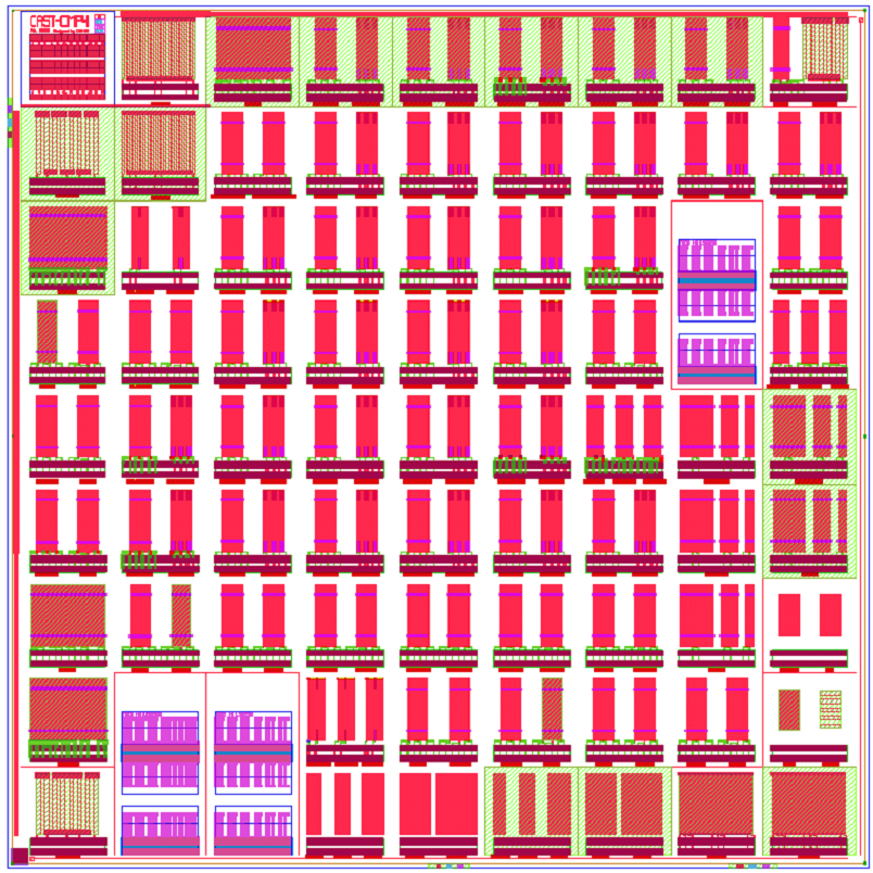
CMP-4 is a standard mask for assessing differences in step height after Cu CMP, using interconnect patterns with different line widths and spaces.
Basic Information
| Item | Details |
|---|---|
| Mask Layout | 20.8mm × 20.8mm |
| Minimum Line Width | 80nm (0.08µm) |
Pattern Dimensions
| Line Width (µm) | Space (µm) |
|---|---|
| 0.08 | 0.08, |
| 0.09 | 0.09, |
| 0.13 | 0.13, |
| 0.18 | 0.18, |
| 0.25 | 0.25, |
| 0.5 | 0.5, |
| 1 | 1, |
| 2.5, | Same as line width (1:1) |
Intermediate dimensions are also available beyond those listed in the table. The mask includes regions with and without dummy patterns, different interconnect lengths, and isolated interconnects with wider spacing from surrounding lines.
Example Film Stack
This is an example wafer structure for Cu CMP testing. Film materials and thicknesses can be discussed to suit your desired structure.
0.6 µm
60 nm
10 nm each
200~300 nm
PT004 | Standard Mask for STI CMP Testing
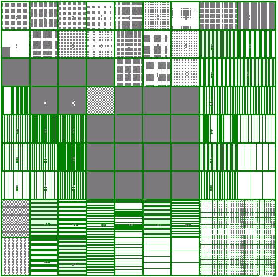
PT004 is a standard mask for CMP testing of STI oxide fill. Regions with different pattern shapes, widths, spaces, and densities allow comparison of step heights after CMP.
Basic Information
| Item | Details |
|---|---|
| Shot Size | 20mm × 20mm |
| Minimum Feature Size | 0.18µm |
Example Patterns
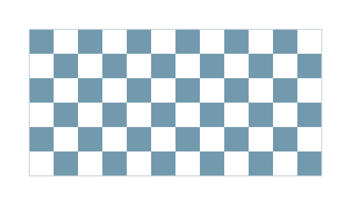
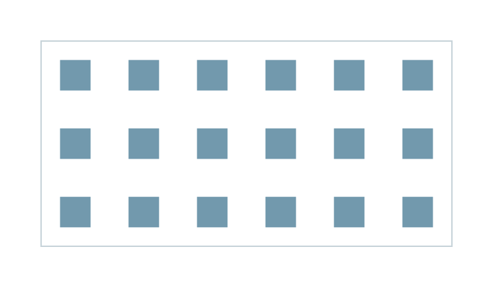
These are plan-view schematics of checker, square, mesh, and line-and-space patterns. Blue areas indicate the patterns.

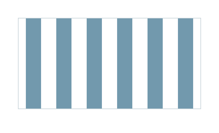
Representative Widths, Spaces, and Densities
| Pattern | Width / Space [µm] (Density) |
|---|---|
| Checker | 1/1, |
| Square | 0.5/0.62(20%), |
| Mesh | 0.2/1.8(19%), |
| Line and Space | 50% Density0.18/0.18, |
| Other Densities5/45(10%), |
Additional width and space combinations are available beyond those listed. Line-and-space densities range from 10~90% in 10% increments, including densities not shown in the table.
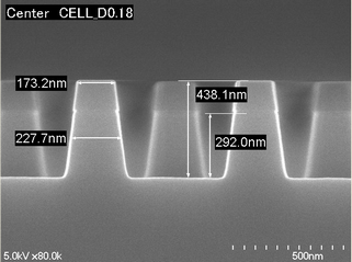
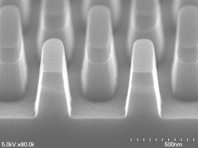
Processing Example | Cross-Sectional SEM after Si Etching
These cross-sectional SEM images show the wafer after Si etching, before oxide fill. Dimensions shown are example measurements at the imaged locations.
754/854 | Standard Masks for Cu CMP Testing
754 and 854 are standard masks for Cu CMP testing. They allow comparison of polishing results across different line widths, spaces, and pattern densities.
| Item | Details |
|---|---|
| Mask | 754/854 |
| Trench Width | 0.18~100 µm |
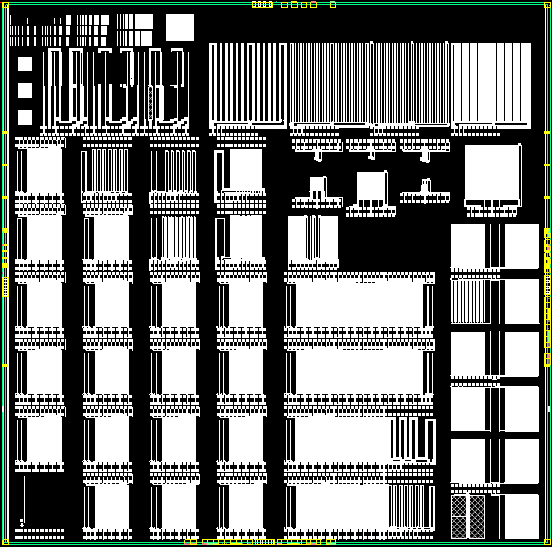
Processing Example after Cu Plating
The photograph below shows an example of a full 754 patterned wafer after Cu plating. It illustrates a processed Cu test wafer; it is not a cross-section after CMP.
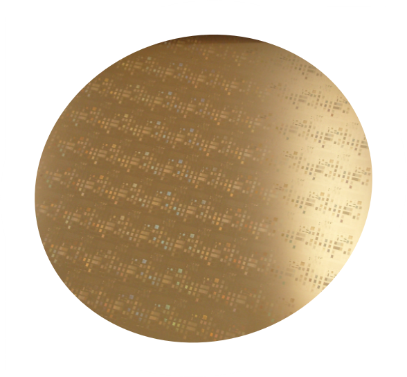
Please let us know your desired structure, including dielectric materials and thicknesses and Cu plating thickness.