
What Is the Charge-Up Monitor?
The Charge-Up Monitor is a test wafer/assessment chip used to assess damage to the gate oxide caused by charging during semiconductor manufacturing processes such as etching, film deposition, and ion implantation. An antenna formed on the chip collects charge during processing, and the structure is such that the collected charge causes damage to the thin gate oxide of a MOS capacitor.
For a processed wafer or chip, I-V characteristics are measured by applying voltage in steps between the Poly-Si gate electrode pad and the backside Si. The effects of charge-up are assessed by comparing the initial and post-process I-V curves. Changes in each I-V curve are also compiled by measurement location (chip position within the wafer) and antenna ratio.
By comparing I-V curves across multiple antenna ratios and measurement locations, trends in oxide damage and differences in sensitivity can be identified. The antenna ratio is the ratio of the Poly-Si antenna electrode area to the active area. The I-V curves and a gate-oxide breakdown-voltage map are provided in Excel.
| Item | Details |
|---|---|
| Available Formats & Sizes | 300 mm / 200 mm / chip: 19.6 mm × 19.4 mm |
| Sales Unit | One or more wafers / one set of four chips |
| Measurement & Result Format | I-V curves / gate-oxide breakdown-voltage map provided in Excel |
| Typical Lead Time to Ship | Approximately one week if in stock |
| Typical Lead Time for Measurement Results | Approximately two weeks after receipt of the processed samples |
Specifications & Product Formats
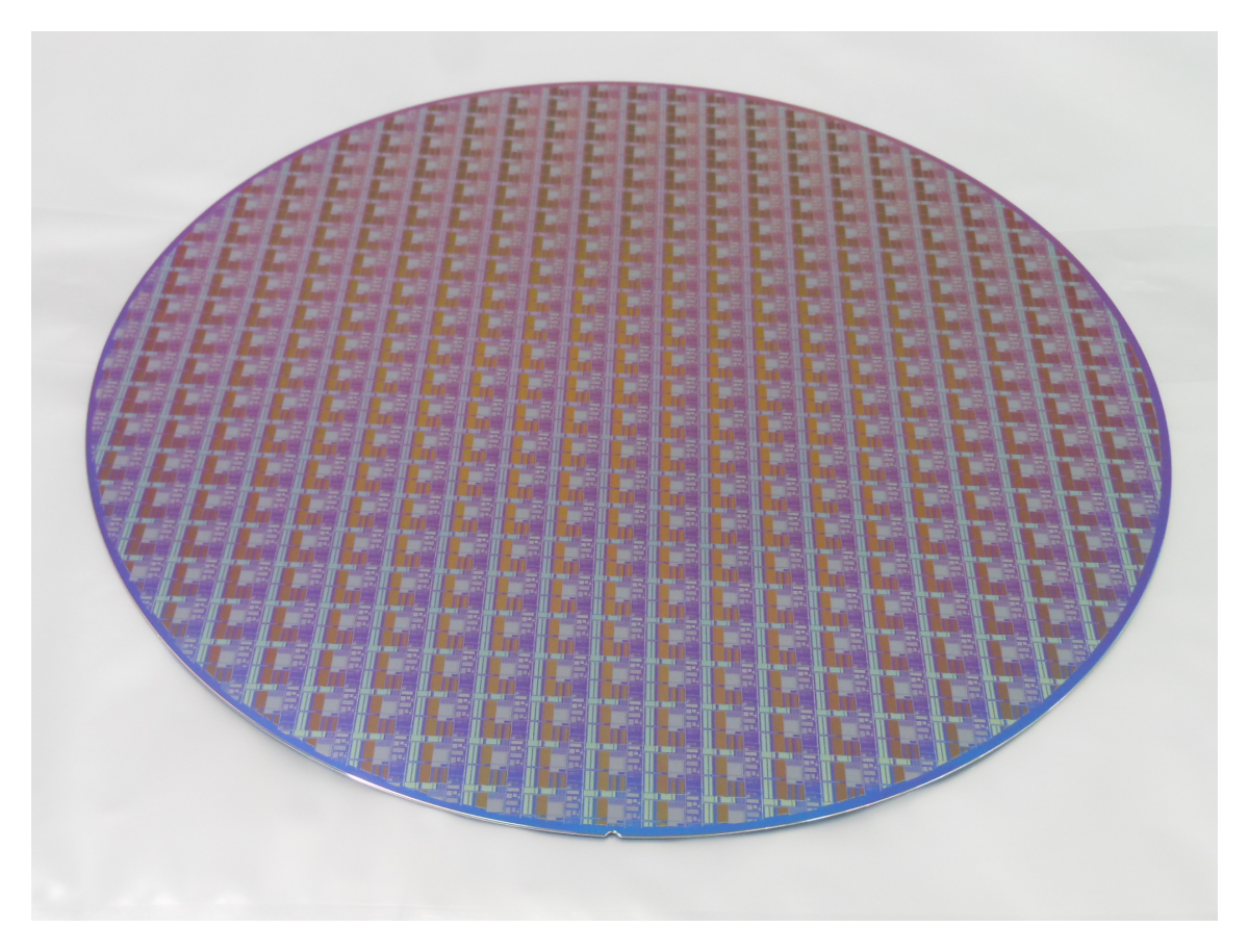
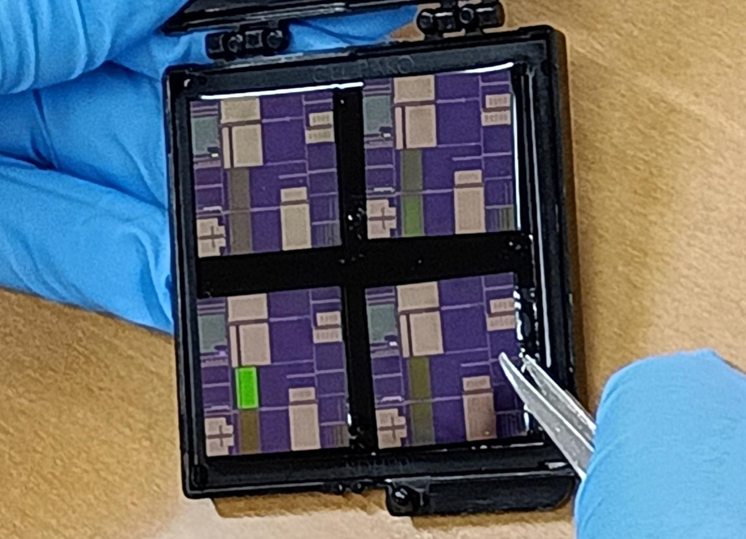
Wafers are available in 300 mm and 200 mm sizes and are sold in quantities of one or more. Chips measure 19.6 mm × 19.4 mm and are sold and measured in sets of four. Using the chip format also makes it possible to assess equipment that handles substrate sizes outside the standard 200 mm/300 mm wafer formats.
The wafer offering includes an electrical measurement service following plasma processing. I-V measurement results for an unprocessed wafer from the same lot, measured immediately after fabrication, can also be provided and used as baseline data for reviewing the post-plasma-process measurement results.
Wafer
Chip
Contact us to discuss the Charge-Up Monitor.
Contact UsProcesses That Can Be Assessed for Charging Damage
Equipment & Process Assessment
The Charge-Up Monitor is a test wafer used to assess plasma-induced charging damage. It is used to assess equipment and processes where charging effects are a concern, including etching, ashing, CVD, PVD, ion implantation, atmospheric-pressure plasma, and drying after cleaning. The initial and post-process I-V curves are compared to identify trends in oxide damage and differences associated with antenna ratio. The breakdown-voltage map is used to check the in-plane distribution of the measurement results.
Potential assessment applications include the following.
- Verification of charging damage during the development of new semiconductor manufacturing equipment
- Condition checks after equipment installation, start-up, modification, or maintenance
- Comparison following changes to process conditions or recipes
- Comparison of trends among multiple tools or chambers
- Identification of wafer locations where damage is concentrated and isolation of the cause
- Periodic monitoring of manufacturing processes and identification of changes from normal conditions
- Investigation of process and yield improvements to reduce degradation of oxide-film reliability
By comparing I-V curves, changes caused by modifications to equipment or process conditions, as well as trends before and after improvements, can be identified. The breakdown-voltage map is used to understand differences among measurement locations across the wafer.
Checking the Within-Wafer Distribution
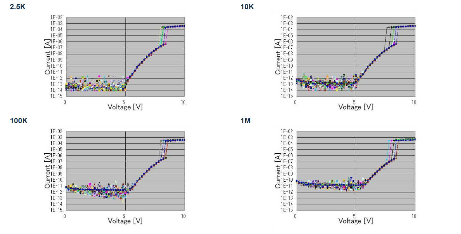
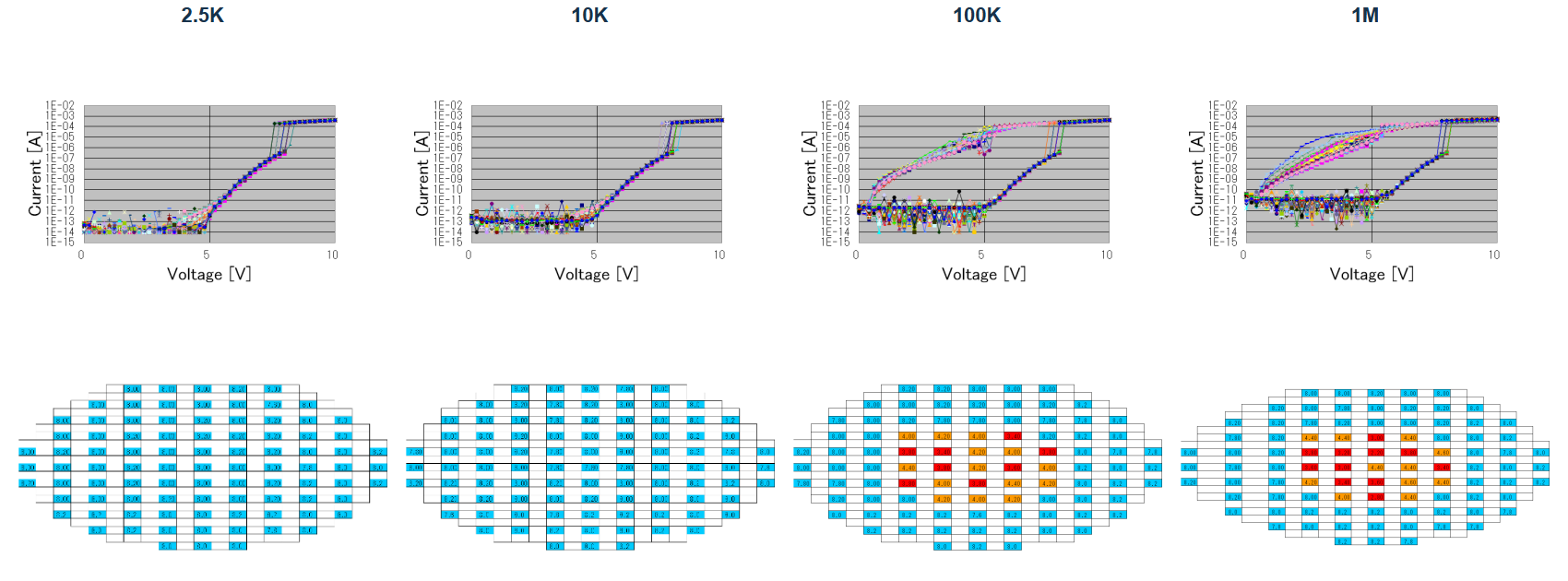
For each I-V curve, the voltage at which the gate oxide breaks down is color-coded and shown on a wafer map. Differences between the wafer center and edge, as well as trends concentrated in specific regions, can be identified from the colors and voltage values.
Checking Sensitivity by Antenna Ratio
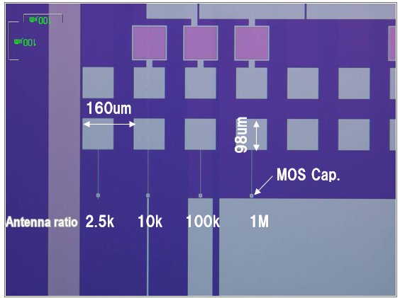
Standard measurements at four antenna ratios—2.5K, 10K, 100K, and 1M—are used to determine differences in sensitivity to charging damage. Patterns with larger antenna ratios collect charge over a larger antenna area for the same gate area and are used for higher-sensitivity assessment.
How Charge-Up Is Assessed Using I-V Characteristics
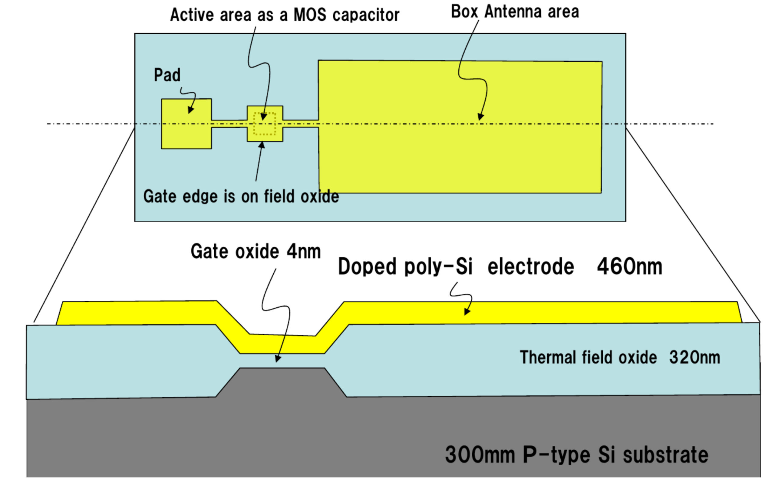
Charge generated by plasma processing and similar processes is collected by the antenna and injected into the gate oxide of the MOS capacitor. In this antenna MOS TEG (Test Element Group: a set of test elements for assessment), current flowing through the oxide increases the number of defects within the film, and when the accumulated damage exceeds a critical level, the leakage current rises sharply, resulting in dielectric breakdown.
In the 300 mm wafer type shown here, devices are isolated by LOCOS, and MOS capacitors are formed using phosphorus-doped Poly-Si electrodes and thermally grown oxide. The cross-sectional structure comprises a 320 nm thermally grown field oxide, a 4 nm gate oxide, and a 460 nm doped Poly-Si electrode. The I-V curves before and after processing are compared to identify the effects of oxide damage, and the breakdown voltage is used to color-code the breakdown-voltage map.
Chip Layouts & Antenna-Ratio Patterns
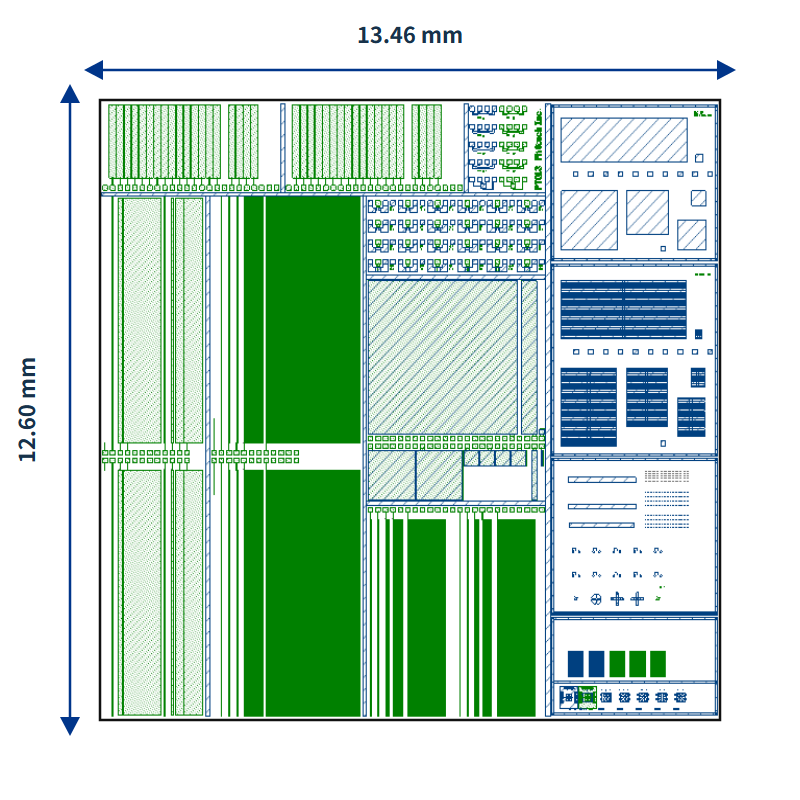
BOX antennas for charge-up assessment are arranged within the chip, and the overall layout shows the locations and configurations of the assessment patterns.
300 mm Chip Layout
200 mm Chip Layout
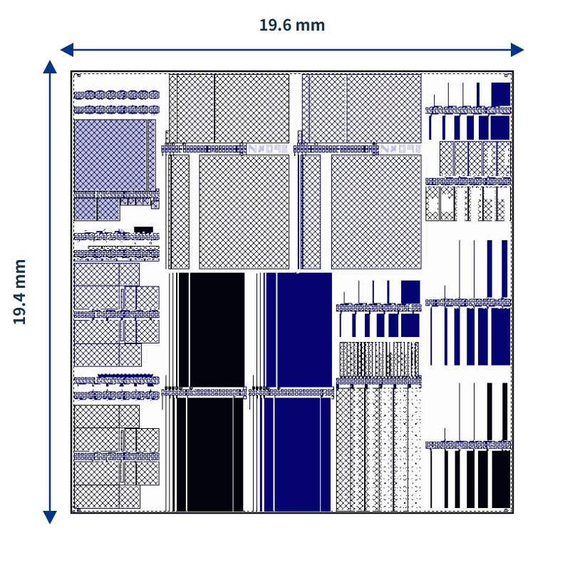
Patterns with various antenna ratios are integrated on the same chip to measure differences in sensitivity to charging damage.
Measurement Method: Workflow for Generating I-V Curves & Breakdown-Voltage Maps
Plasma-processed samples are measured in four steps: sample setup, electrode connection, acquisition of I-V characteristics, and compilation of results.
- Preparation
Load the Sample
Load the plasma-processed wafer or chip onto the probe station. - Connection
Connect the Electrodes
Connect the Poly-Si gate electrode pad as the negative electrode and the backside Si as the positive electrode. - Measurement
Acquire I-V Characteristics
Measure the current while increasing the applied voltage stepwise. - Compilation
Compile the Results in Excel
Compile the I-V curves and the breakdown-voltage map, color-coded by measurement location.
The voltage at which the current flowing through an active area of 4 µm² exceeds 1 µA is defined as the breakdown voltage, and a map of this breakdown voltage (withstand voltage) is displayed for each measured chip position. Assessment is performed using this map and the I-V curves. In the standard measurement of a 300 mm wafer, approximately 25% of the valid chips are typically selected in a checkerboard pattern for measurement.
Assessment Examples & Measurement Locations
The Excel file contains I-V curves for each measurement location and a breakdown-voltage map in which the breakdown voltage extracted from each curve is color-coded. Assessment examples are shown for 300 mm, and standard measurement locations are illustrated for 200 mm.
300 mm: Initial Measurement Results & Two Process Assessment Examples
The figures shown for 300 mm present the initial measurement results, together with assessment examples 1 and 2 after plasma processing, for each of the 2.5K, 10K, 100K, and 1M antenna ratios.
In the post-process assessment examples, differences in the I-V curves among antenna ratios are compared. The breakdown-voltage maps are used to check in-plane trends by measurement location.
Initial Measurement Results
Assessment Example 1
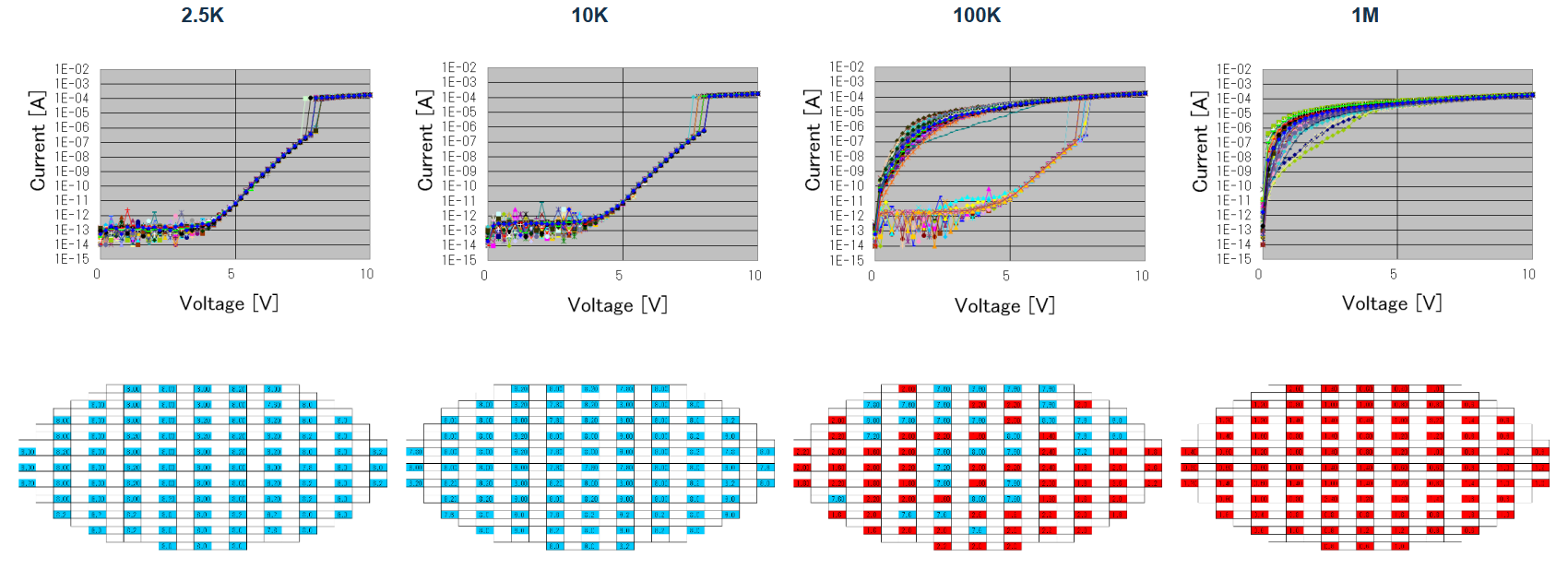
Assessment Example 2
Measurement Locations for 200 mm

Workflow & Typical Lead Times from Order to Delivery of Excel Measurement Data
The process consists of six steps, from confirmation of specifications through delivery of the assessment results.
Specification Confirmation
Confirm the wafer diameter, wafer or chip format, and process to be assessed.
Shipping
Ship the wafer or chips. In-stock items typically ship in approximately one week.
Plasma Processing
The customer carries out plasma processing.
Return Shipment
Return the processed wafer or chips.
I-V Measurement
Measure the I-V curves of the returned samples, with assessment focused on the I-V curves.
Results Delivery
Provide the I-V curves and breakdown-voltage maps in Excel. The typical lead time is approximately two weeks after receipt of the samples.
Shipping and measurement lead times vary depending on inventory status, specifications, and schedule. Because the customer’s processing time and transportation time are not included, the total lead time will be communicated separately for each case.
Purchasing, Quotations, & Technical Consultation for the Charge-Up Monitor
For purchase or quotation inquiries, you can contact us even before the size or wafer/chip format has been determined. When contacting us, please provide an overview of the assessment, including the assessment objective, target process, and requested delivery date, to the extent possible. The four standard antenna ratios measured are 2.5K, 10K, 100K, and 1M; other antenna ratios can also be measured upon request.