Philtech Support
Stock products can typically be shipped within one week.
We can reuse an existing mask, create a new mask, or perform photomask-free exposure using a direct-write lithography system. We can then use etching to form trench patterns, hole patterns, and other structures. We can handle wafer sizes from 4 to 12 inches as well as individual chips.
Philtech offers both stock products and new custom processing services.
Dimensional terminology: For PT063, trench width refers to the mask dimension. For the 6-inch product, trench width refers to the finished dimension after processing. Mask dimensions and finished dimensions are different.
What Is a Trench Pattern Wafer?
A trench pattern wafer is a test wafer patterned with groove-shaped structures. It is used to evaluate film coverage, gap-fill characteristics, and related properties.
By observing films formed on the top surface, sidewalls, and bottom of a trench cross section, you can evaluate conformality and step coverage. Structures with different widths and depths also enable comparison of film deposition on high-aspect-ratio structures.
Differences in film thickness and film quality among the top surface, sidewalls, and bottom can be compared under deposition conditions such as pressure, temperature, precursor supply time, gas flow rate, purge time, and plasma conditions.
The relationship between step coverage and conditions such as pressure, temperature, and applied power can be examined.
Cross-sectional observation can reveal growth from the trench bottom, deposition on the sidewalls, seams and voids, and the fill profile inside the trench.
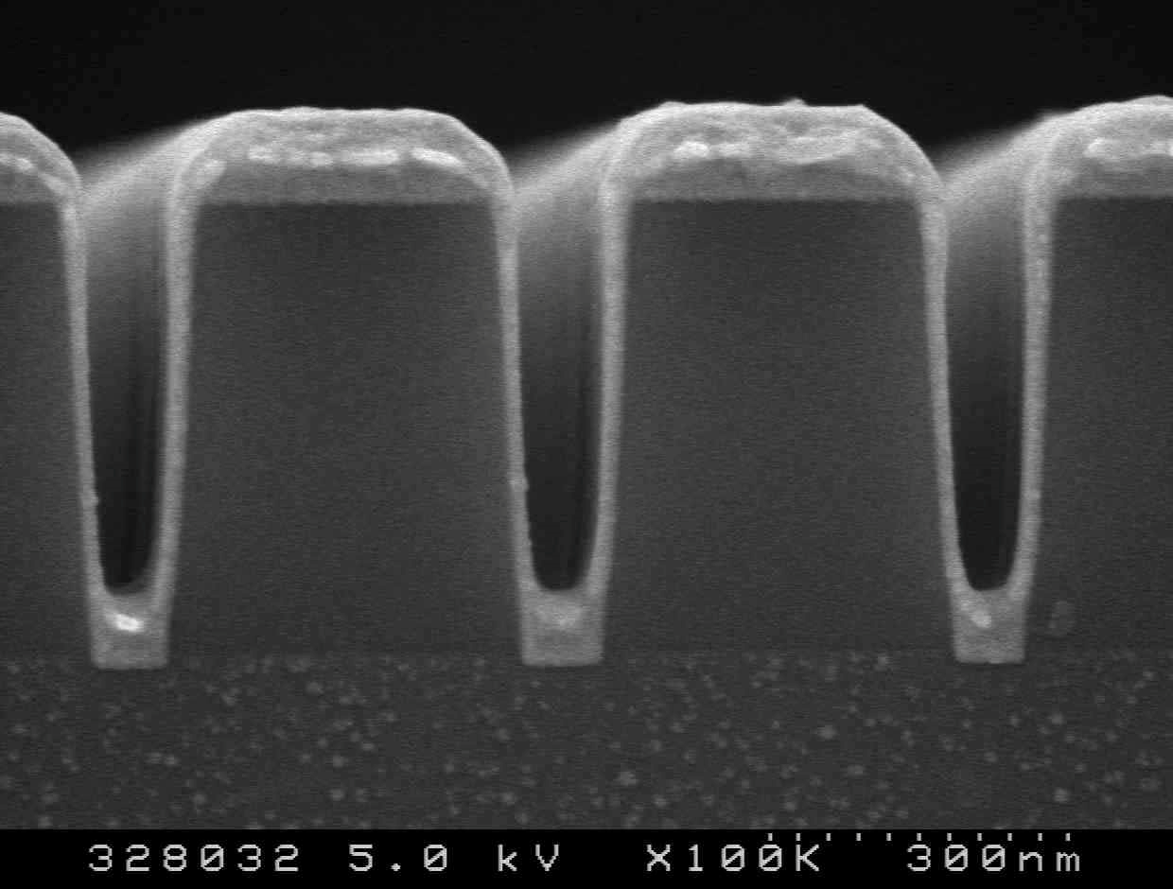
Evaluation Case | PVD-Cu Film Coverage
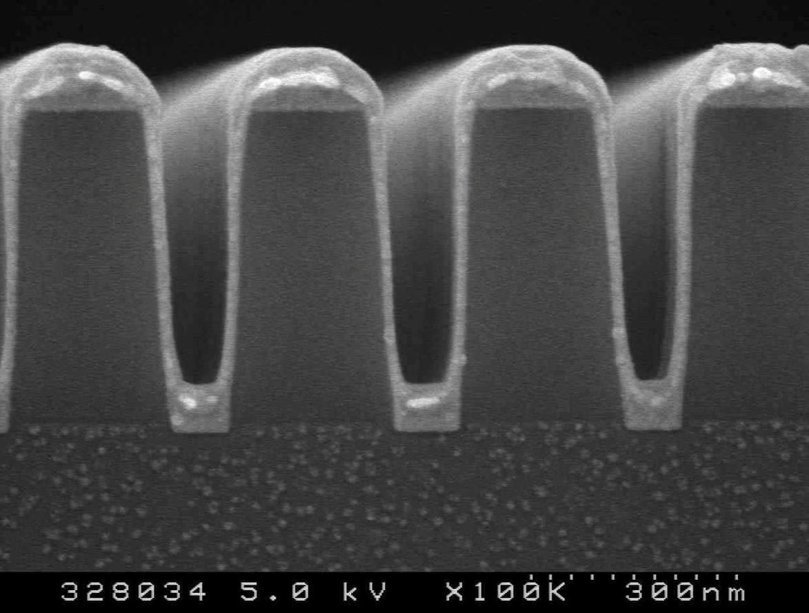
This is an example of evaluating PVD-Cu film coverage using a TEG fabricated by Philtech.
Discuss specifications and processing conditions with us.
Contact Us8-Inch Trench Pattern Wafer (PT063)
This product has trenches formed in a 200 mm-diameter silicon wafer by Bosch DRIE (Si etching) using a silicon oxide hard-mask process. It has mask dimensions ranging from 0.2 µm to 10 µm, with multiple pattern groups of different widths, spacings, and trench counts arranged within each chip. In addition to the standard specification, custom production with a modified trench depth is available for consultation.
Basic Information
| Item | Specification |
|---|---|
| Wafer size | 8 inches (200 mm) |
| Wafer orientation feature | Notch |
| Mask name | PT063 |
| Chip size | 18 mm square |
| Mask dimensions | 0.2 µm to 10 µm |
| Trench length | 3.5 mm |
| Process | Bosch DRIE |
| Available formats | 8-inch wafer / 18 mm square chip |
Pattern Arrangement and Shot Layout
PT063 Group Placement
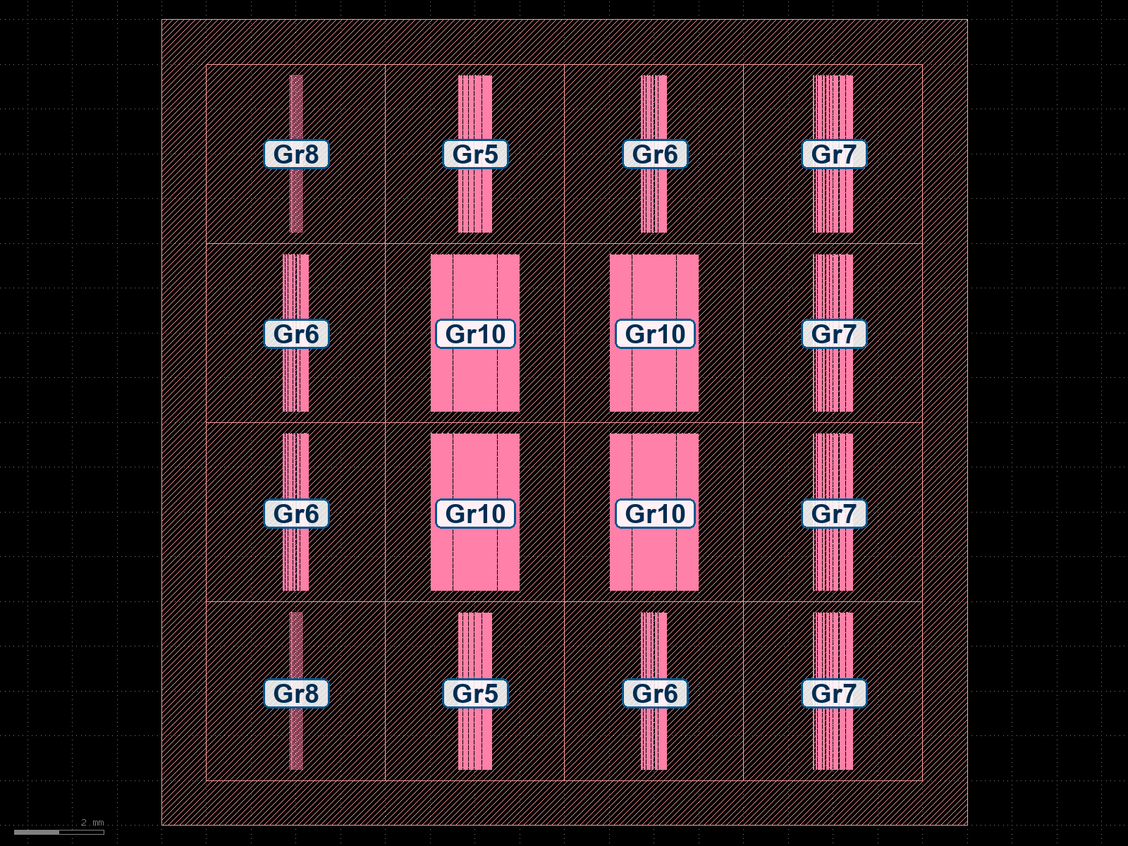
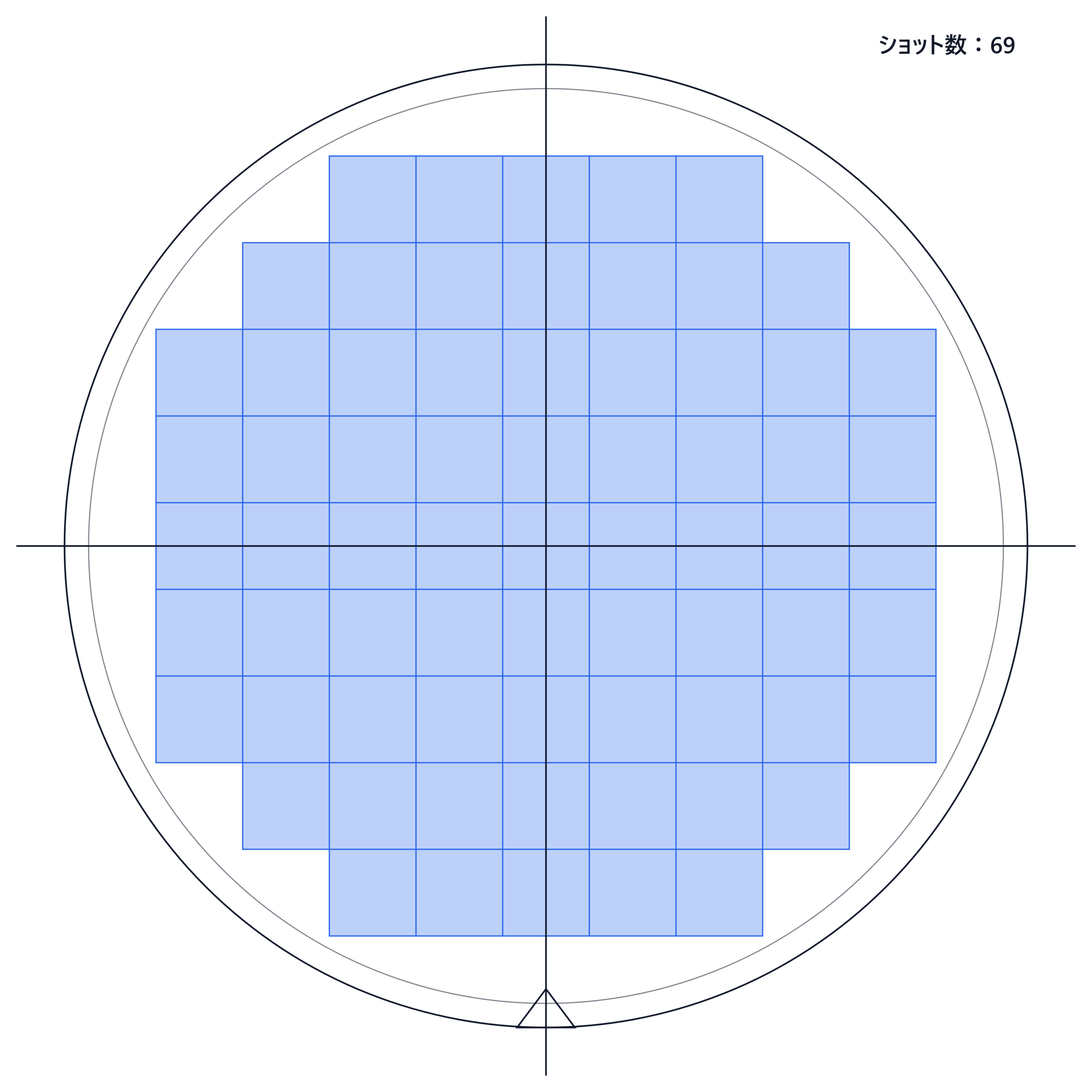
PT063 Shot Map
PT063 Widths, Spacings, and Trench Counts
Each dimensional pair in the table is listed in the order trench width / spacing to the adjacent trench (edge-to-edge distance). The second value is not the center-to-center pitch. For example, “0.4 µm / 1.2 µm” means a trench width of 0.4 µm, an edge-to-edge spacing of 1.2 µm, and a center-to-center pitch of 1.6 µm.
| Group | Trench width (mask dimension) / spacing | Trench count and arrangement |
|---|---|---|
| Gr5 | 0.4 µm / 1.2 µm, 0.5 µm / 1.5 µm, 0.6 µm / 1.2 µm, 1 µm / 2 µm, 2 µm / 2 µm | 50 trenches each |
| Gr6 | 0.2 µm / 1.2 µm, 0.25 µm / 1.25 µm, 0.3 µm / 1.2 µm, 0.35 µm / 1.4 µm, 0.4 µm / 1.6 µm, 0.5 µm / 2 µm, 0.6 µm / 2.4 µm, 1 µm / 4 µm | 20 trenches each |
| Gr7 | 0.2 µm / 1.8 µm, 0.25 µm / 2.25 µm, 0.3 µm / 2.7 µm, 0.35 µm / 3.15 µm, 0.4 µm / 3.6 µm, 0.5 µm / 4.5 µm, 0.6 µm / 5.4 µm, 1 µm / 9 µm, 2 µm / 11 µm, 5 µm / 10 µm | 10 trenches each |
| Gr8 | 0.2 / 0.25 / 0.3 / 0.35 / 0.4 / 0.5 / 0.6 / 1 / 2 / 5 µm | 30 µm spacing |
| Gr10 | 1 µm / 4 µm, 2 µm / 5 µm, 5 µm / 7 µm, 10 µm / 10 µm | 20, 20, 10, and 5 trenches, respectively / repeated four times |
Unit: µm / Trench length: 3.5 mm
Manufacturing Example: Results from Cross-Sectional SEM Observation
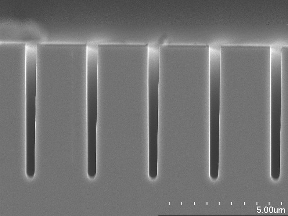
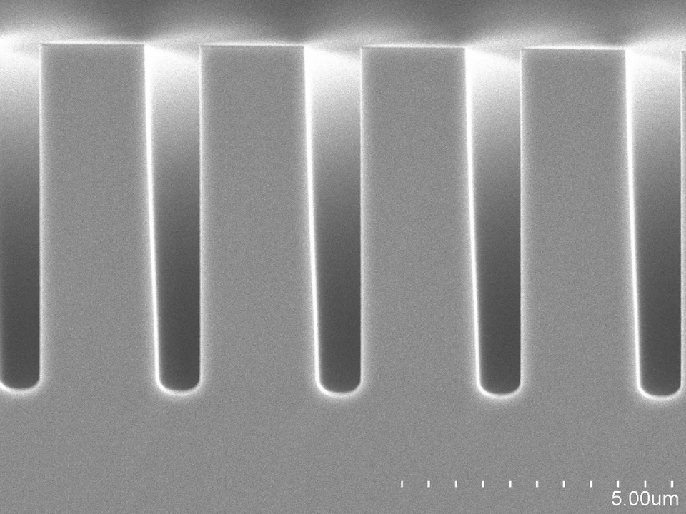
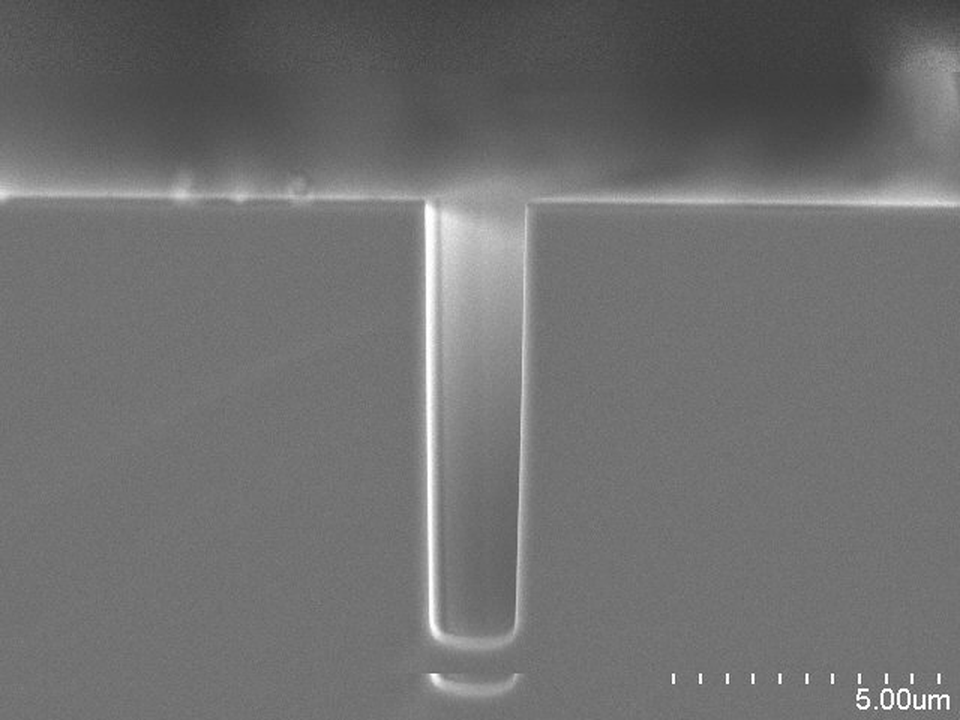
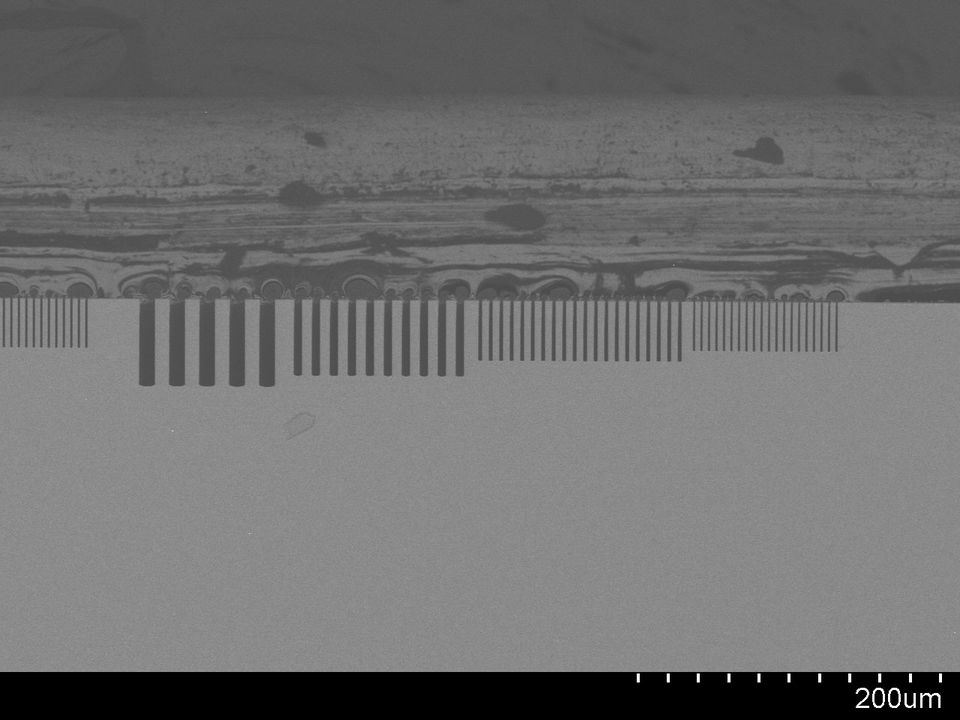
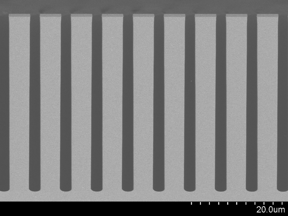
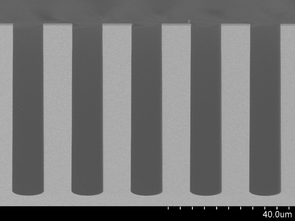
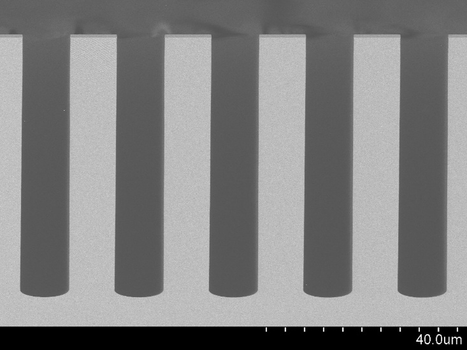
These processing results were obtained by cross-sectional SEM observation of a chip at the wafer center and a chip near the wafer edge. Depth, top width, and middle width were measured in the 3.5 mm-long trench region.
Measurement Results
Wafer Center
| Mask dimension | Depth | Top width | Middle width |
|---|---|---|---|
| 0.2 | 20.7 | 0.49 | 0.59 |
| 0.25 | 22.0 | 0.49 | 0.66 |
| 0.3 | 22.9 | 0.49 | 0.70 |
| 0.35 | 23.9 | 0.53 | 0.75 |
| 0.4 | 24.8 | 0.67 | 0.81 |
| 0.5 | 26.3 | 0.82 | 0.92 |
| 0.6 | 27.5 | 0.90 | 1.02 |
| 1.0 | 31.6 | 1.24 | 1.41 |
| 2.0 | 38.5 | 2.01 | 2.40 |
| 5.0 | 49.1 | 4.97 | 5.33 |
| 10 | 56.5 | 9.80 | 10.21 |
Unit: µm
Wafer Edge
| Mask dimension | Depth | Top width | Middle width |
|---|---|---|---|
| 0.2 | 19.6 | 0.46 | 0.57 |
| 0.25 | 20.8 | 0.44 | 0.61 |
| 0.3 | 21.8 | 0.43 | 0.65 |
| 0.35 | 22.7 | 0.44 | 0.71 |
| 0.4 | 23.5 | 0.56 | 0.75 |
| 0.5 | 25.1 | 0.71 | 0.85 |
| 0.6 | 26.3 | 0.81 | 0.93 |
| 1.0 | 30.4 | 1.12 | 1.30 |
| 2.0 | 37.3 | 1.97 | 2.23 |
| 5.0 | 47.3 | 4.92 | 5.13 |
| 10 | 54.4 | 9.85 | 9.98 |
Unit: µm
Cross-Sectional SEM Images from the Wafer Center and Edge
Note: The cross-sectional SEM images were taken before removal of the silicon oxide hard mask. Product wafers are shipped after the silicon oxide hard mask has been removed.
Low Magnification
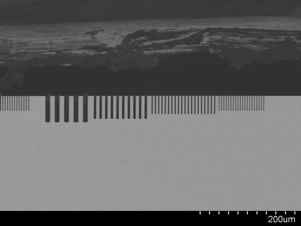
0.2 µm Mask Dimension
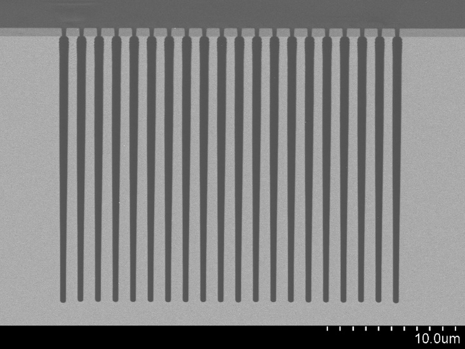
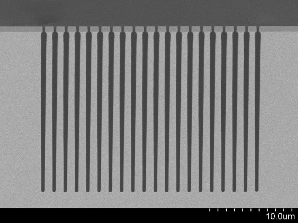
0.5 µm Mask Dimension
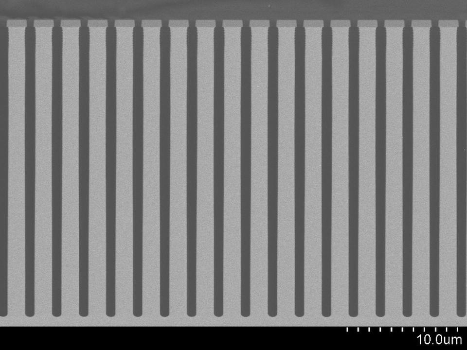
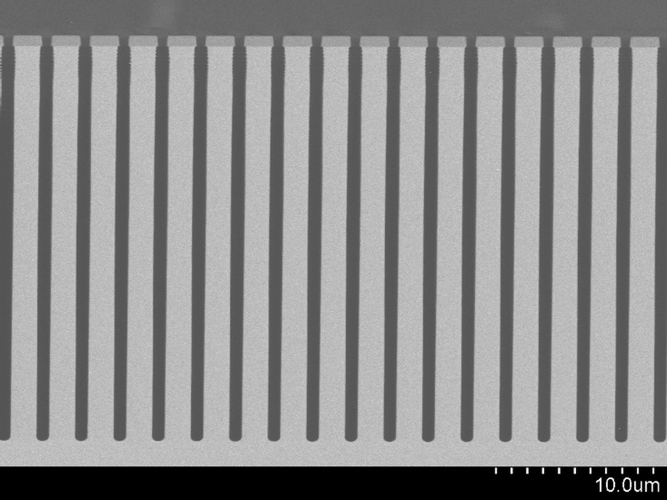
2 µm Mask Dimension
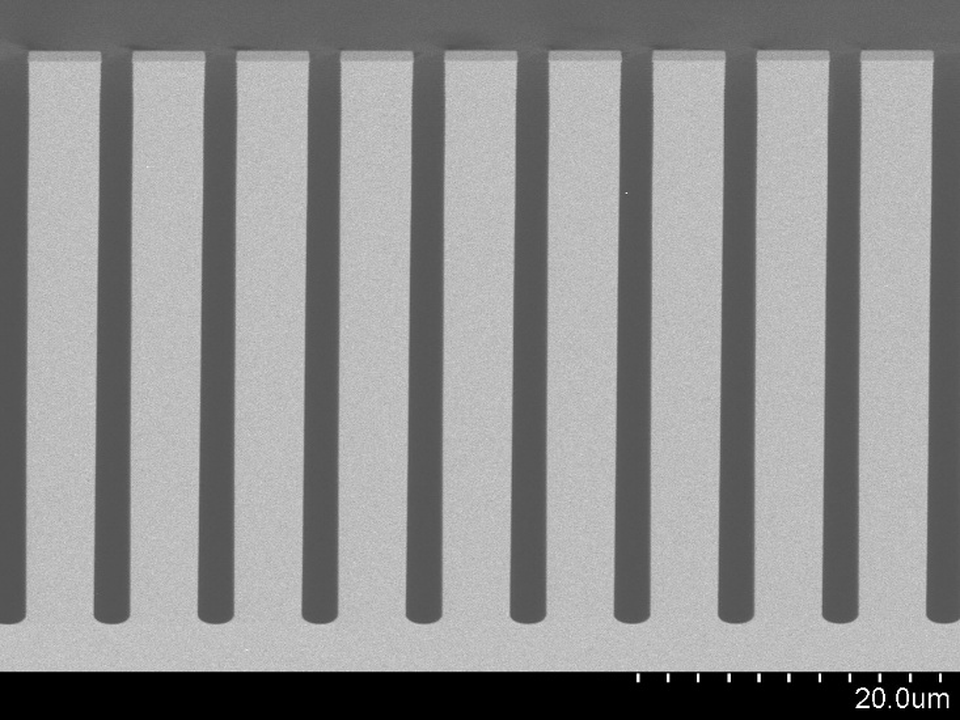
10 µm Mask Dimension
6-Inch Trench Pattern Wafer
This product has trenches with finished dimensions of 0.5 µm, 1 µm, and 2 µm formed in a 150 mm-diameter silicon wafer by non-Bosch Si etching. These trenches, which do not have the periodic sidewall scalloping produced by Bosch DRIE, can be used for evaluation.
Basic Information
| Item | Specification |
|---|---|
| Wafer size | 6 inches (150 mm) |
| Wafer orientation feature | JEITA orientation flat (length: 47.5 ± 2.5 mm) |
| Trench width (finished dimension) | 0.5 µm, 1 µm, 2 µm |
| Process | Non-Bosch Si etching |
| Available formats | 6-inch wafer / approximately 15 mm square chip |
| Chip configuration | Three regions for each finished dimension (0.5 µm, 1 µm, and 2 µm), for a total of nine regions. |
Manufacturing Example: Results from Cross-Sectional SEM Observation
| Trench width (finished dimension) | Depth after processing |
|---|---|
| 0.5 µm | 5.2 µm |
| 1 µm | 6.5 µm |
| 2 µm | 7.6 µm |
Shot Layout and Dicing Lines
This shot layout contains regions with finished dimensions of 0.5 µm, 1.0 µm, and 2.0 µm. The red dashed lines indicate the dicing lines for an approximately 15 mm square chip containing three regions of each dimension, for a total of nine regions.

Cross-Sectional SEM Images from the Manufacturing Example